In the field of process technology and characterization, process sequences and individual process steps for the manufacture of innovative semiconductor devices are developed, characterized, and optimized. The aim is to gain a comprehensive understanding of the relationship between process parameters, material properties, and device performance. One focus is on the development of processes for the realization of reliable, high-temperature-resistant, and efficient devices for demanding power, high-temperature, and sensor applications on semiconductors with high and ultra-high band gaps.
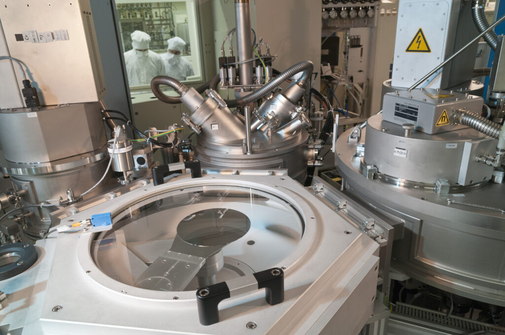
To this end, the chair, in cooperation with the Fraunhofer Institute for Integrated Systems and Device Technology (IISB), has access to complete process lines for silicon and silicon carbide in the FAU’s clean room laboratory with extensive analysis and measurement technology.
Current research topics:
- Physical modeling of microspectroscopic measurements for the characterization of thin-film systems (Julian Schwarz)
- Development of electron and radiation detectors, including readout electronics based on (U)WBG sensors (Gordon Neue, Yujia Liu)
- Epitaxial growth for 2-dimensional hole gases in III/IV semiconductor systems for functionalization in power electronic components (doctoral project in cooperation with Fraunhofer IISB)
- Alternative approaches for the production and characterization of ohmic contacts on p- and n-type silicon carbide (doctoral project in cooperation with Fraunhofer IISB)
- Multilayer metallization for high-temperature-stable 4H-SiC-CMOS devices (doctoral project in cooperation with Fraunhofer IISB)
- Development of robust lithography processes for sub-micrometer technology on 4H-SiC (doctoral project in cooperation with Fraunhofer IISB)
Contact
Dr.-Ing. Norman Böttcher
Research associates